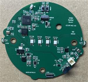
The power and ground planes form the backbone of a stable and efficient PCB design. The ground plane acts as a common reference point for all electrical signals and provides a low-impedance return path for current. The power plane, on the other hand, distributes supply voltage evenly to components across the board, helping minimize voltage drop and ensuring stable operation.
Together, they serve as an integrated solution for the power distribution network (PDN), signal return path, impedance control, distributed capacitance, and EMI shielding. From a performance perspective, well-designed planes directly determine power integrity and signal quality by maintaining low impedance, minimizing loop areas, and ensuring continuity throughout the board.
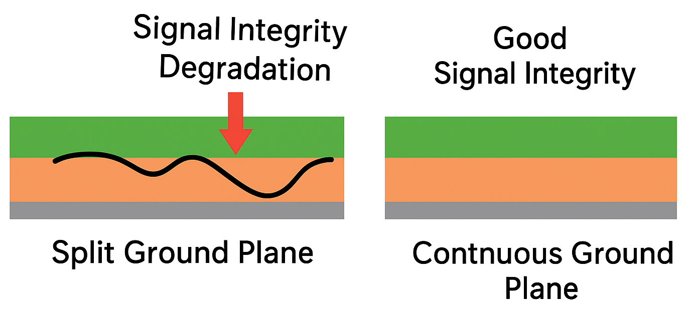
Poor power and ground plane design can lead to serious power integrity and signal integrity problems.
Below are several typical issues:
This is one of the most common — and most dangerous — design mistakes.
While it might not matter for low-speed signals, in high-speed digital systems, signals rely on their reference plane as a current return path.
When that reference plane is broken or split, several problems occur:
Solutions:

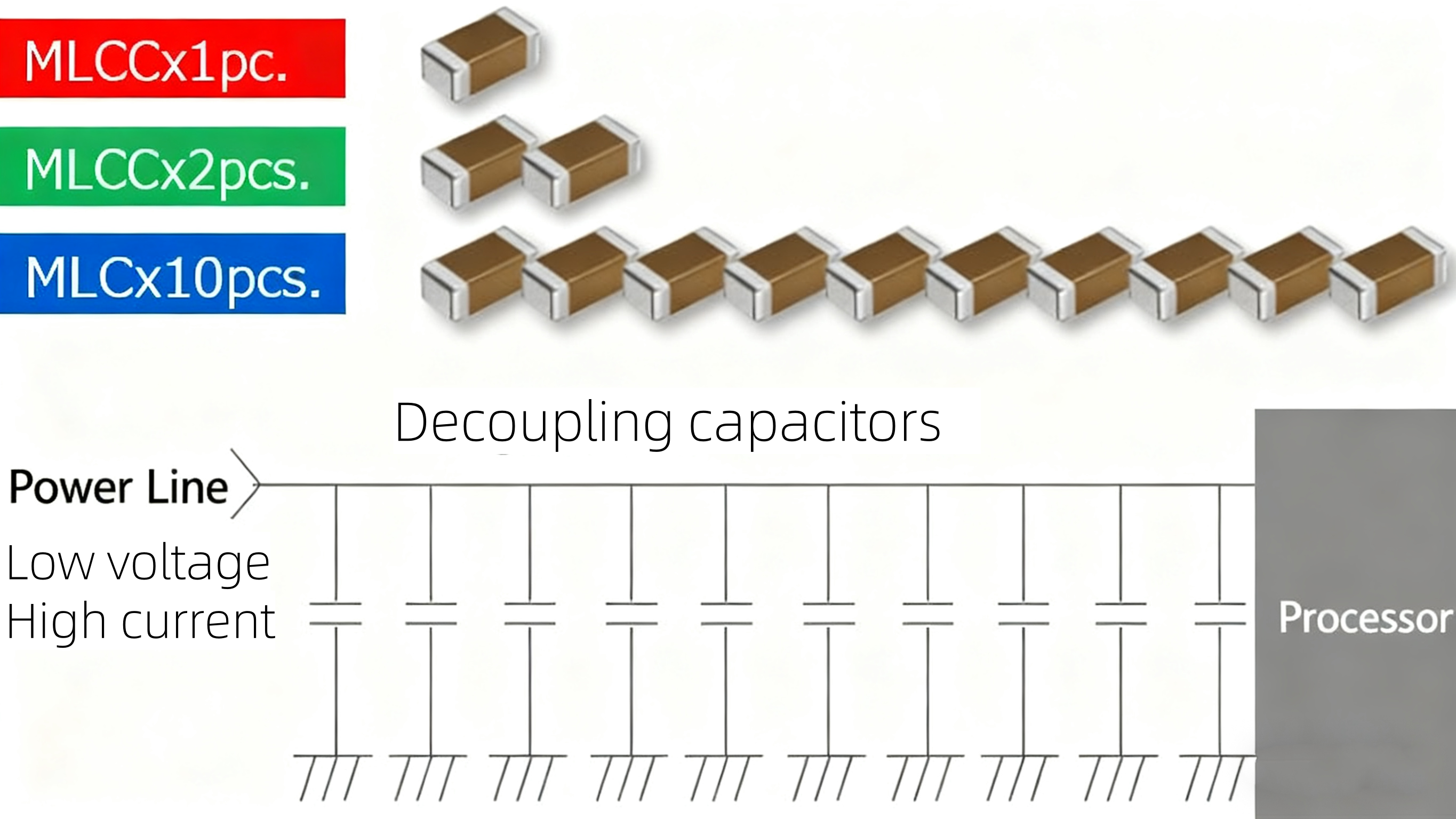
If the impedance of the power distribution network (PDN) viewed from a chip’s power pin is too high within its operating frequency range, transient current demand can cause sudden voltage dips.
Solutions:
The allocation of power and ground planes is the core of PCB stack-up design, directly determining the circuit’s performance, EMC characteristics, and overall cost.
The ground plane acts as the system’s “earth” — a universal reference point for all signals. It must be the most stable and complete plane in your PCB stack-up.
In any multilayer PCB, ensure at least one continuous ground plane layer.
Even in a 4-layer board, if you can’t afford a full power plane, you should always maintain a complete ground plane.
Never split the ground plane — breaks in the return path can severely compromise signal integrity.
If you must separate analog and digital domains, do it through layout isolation, not plane segmentation.
Critical high-speed signal layers (like clocks or differential pairs) should always be placed next to a ground plane, not a power plane.
Minimizing current loop area is key to controlling EMI noise, crosstalk, and power noise.
Always arrange power and ground planes as adjacent layers. Use thin dielectric material (0.1–0.2 mm) between them to increase plane capacitance, which enhances high-frequency decoupling.
Every signal layer must have a continuous reference plane beneath or above it — preferably a ground plane, secondarily a power plane. This guarantees a clear and low-inductance return path for the signal current.
Consistent impedance is crucial for preventing signal reflection and maintaining signal integrity.
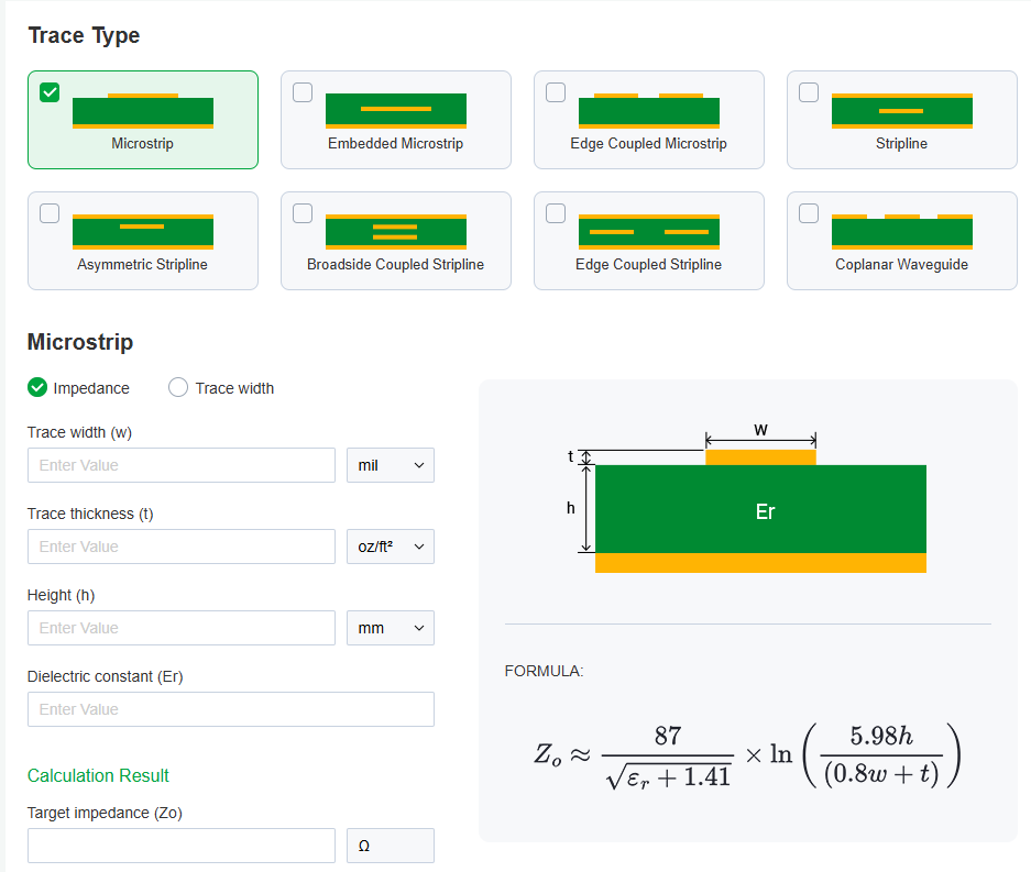
A continuous plane is essential for accurate impedance calculation.
Gaps or splits under the trace make impedance unpredictable, causing reflections and distortion.
Use an impedance calculator to determine appropriate dielectric thickness, trace width, and spacing during the PCB stack-up design phase.
The following examples illustrate the most common stack-up structures used in 4-layer, 6-layer, and 8-layer PCBs.
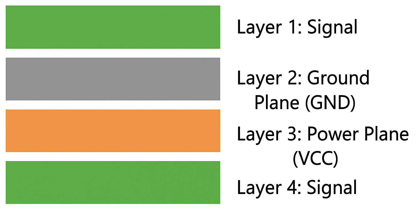
4-Layer PCB
Layer 1: Signal 1
Layer 2: GND
Layer 3: Power
Layer 4: Signal 2
Advantages: Highly recommended structure. Both signal layers have solid ground reference planes. The power and ground planes are tightly coupled, improving distributed capacitance and power integrity.
Disadvantages: The power plane is relatively far from the top signal layer — impedance control must be carefully managed for high-speed traces.
6-Layer PCB
Option 1: Signal Integrity Priority
Layer 1: Signal 1
Layer 2: GND
Layer 3: Signal 2
Layer 4: Power
Layer 5: GND
Layer 6: Signal 3
Advantages:
Disadvantages: Impedance calculation for S2 is more complex since it’s between two different reference planes.
Option 2: EMC & Power Integrity Priority
Layer 1: Signal 1
Layer 2: GND
Layer 3: Signal 2
Layer 4: Signal 3
Layer 5: Power
Layer 6: GND
Advantages:
Disadvantages: S3 uses the power plane as a reference; if that plane contains multiple voltages or noise, it can affect signal quality.
8-Layer board
Layer 1: Signal 1
Layer 2: GND
Layer 3: Signal 2
Layer 4: Power
Layer 5: GND
Layer 6: Signal 3
Layer 7: GND
Layer 8: Signal 4
Advantages:
Disadvantages: Higher manufacturing cost
Power and ground planes are far more than just “copper pours” — they are the foundation of high-speed PCB design. A well-designed plane structure serves not only as a conductor but also as the electrical and structural backbone of the entire board. Proper power and ground plane layout enhances stability, reduces noise, and preserves signal integrity.
In the end, understanding and carefully planning the relationship between power and ground planes is what separates a functional PCB from a truly reliable one.
Feel free to contact us if you have any question.