PCB layout is the process of converting a circuit schematic into a manufacturable PCB design. A high-quality PCB layout ensures the functionality, reliability, and performance of the final product while reducing costs and production risks. Below is a step-by-step overview of the PCB layout design process we follow.
The first stage of PCB design is preparation. Our engineers review the schematic provided by the client to confirm whether it is ready for layout. We check the completeness of component information and verify important PCB requirements such as board size, number of layers, and design constraints.
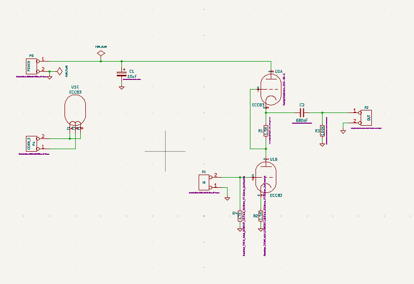
If the client only provides a PDF or image schematic, we will redraw it in professional EDA software.
If the source schematic file is available, we directly generate the netlist and move on to the layout stage.
This step ensures a strong foundation for a smooth PCB layout process.
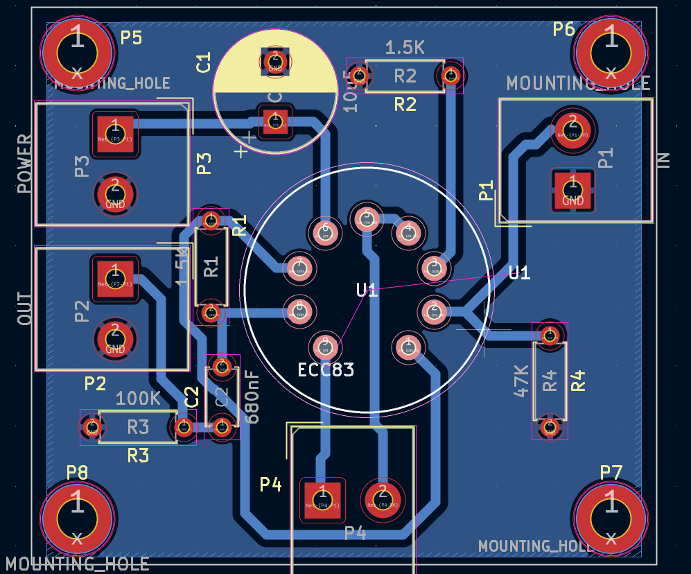
The second step of PCB layout is component placement, which plays a critical role in ensuring both performance and manufacturability of the circuit board. In this stage, all components—such as ICs, resistors, capacitors, and connectors—are positioned logically on the PCB.
During placement, we carefully consider signal flow, thermal management, and electromagnetic interference (EMI) to reduce noise and improve stability.
A well-optimized PCB component placement not only makes the subsequent routing process smoother but also improves signal integrity, heat dissipation, and overall PCB reliability.
PCB routing (also called trace routing) is the process of connecting all components with copper traces according to the schematic. This stage requires precision and is often the most time-consuming step in PCB design.
Proper routing ensures high-speed performance, reduced signal interference, and compliance with manufacturing standards.
After routing is complete, we refine and verify the layout through post-processing steps:
This stage guarantees that the PCB layout meets both electrical and mechanical requirements.
We will send the layout file to client to reivew. Once the design is approved, we generate Gerber files, which are the standard output format for PCB manufacturing. These files include:
By delivering Gerber files along with BOM and drill data, we ensure the PCB can be fabricated by any professional manufacturer.
The final step is PCB manufacturing. With Gerber files, drill data, and BOM, the PCB manufacturer fabricates the physical board. A high-quality PCB layout file ensures smooth production, minimizes risks, and helps achieve faster time-to-market.
PCB layout design is much more than just drawing traces. It requires systematic planning, professional knowledge, and strict verification to guarantee that the final PCB is manufacturable, reliable, and high-performing.
If you have any question of layout, feel free to contact us.


