Thermal management in modern PCB design is a critical factor that directly impacts product performance, reliability, and lifespan.
As electronic products continue to become more compact and integrate more functionality, thermal challenges in PCB layout have increased significantly.
If the heat generated on a PCB cannot be efficiently dissipated, it may lead to severe issues such as component performance degradation, signal integrity deterioration, and even system failure. Therefore, a good PCB layout design must achieve a balanced integration between electrical performance and thermal management.
Heat generation in PCBs mainly comes from the following sources:
High-power components convert a portion of electrical energy into heat during operation, making them the primary focus in PCB layout thermal management.
As current flows through traces, vias, and copper planes, resistance causes Joule heating, which contributes to overall PCB heat dissipation.
In high-frequency circuits such as DC-DC converters or PWM drivers, charging/discharging losses and cross-conduction losses create significant heat.
High-density integrated chips generate heat through constant transistor switching. Effective thermal conduction through pads, vias, or copper pours is required.
PCBs placed in confined enclosures or near heat sources (like motors or power supplies) experience elevated ambient temperatures, reducing overall heat dissipation efficiency.
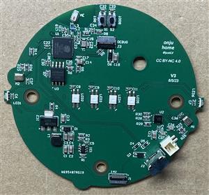
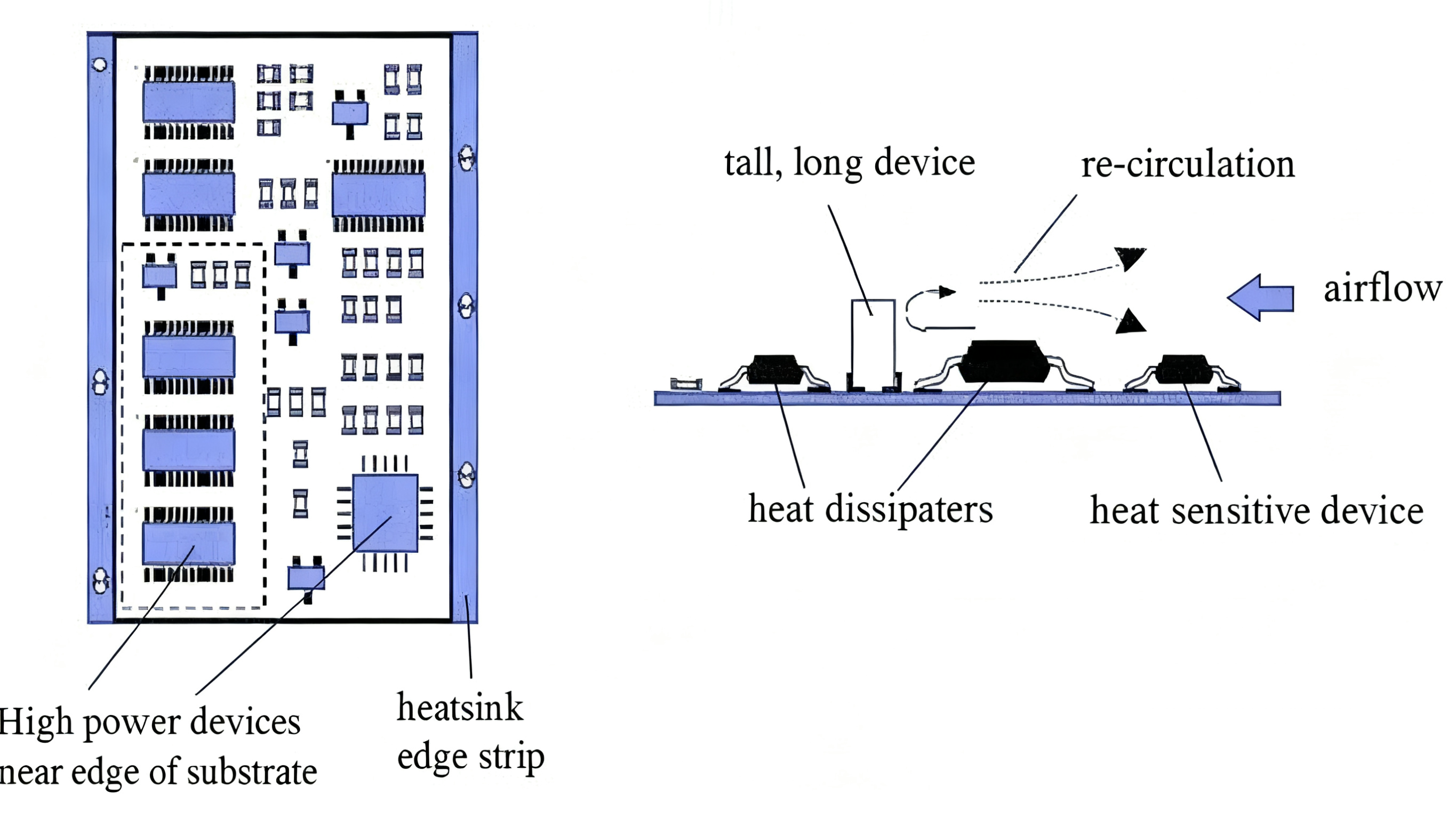
Component layout plays a vital role in PCB heat dissipation. Proper placement can greatly reduce local hot spots and improve the board’s thermal balance.
Avoid clustering multiple high-power components (CPU, MOSFETs, power ICs) in one area. Instead, distribute high-power components across the board to maximize surface area for heat dissipation. Splitting a large heat source into smaller distributed sources lowers local thermal density, improving overall PCB thermal management.
Temperature-sensitive components can suffer performance degradation and reduced lifespan under prolonged high temperatures. In smart PCB design, separate high-temperature and low-temperature zones, and provide physical gaps or buffer components to isolate sensitive devices.
Placing a high-power IC in an area without internal copper connections or far from mounting holes may prevent heat from being effectively conducted away. For effective thermal design in PCB, locate high-power devices near PCB edges or mounting holes, and use wide traces or copper pours to connect power pins for better heat conduction.
Copper is an excellent thermal conductor, and a well-designed copper layout can significantly reduce local temperature and distribute heat more evenly across the board.
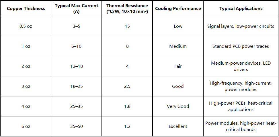
The thicker the copper, the better the heat conduction performance. For high-power circuits, using copper thicknesses of 2 oz or more can significantly improve heat dissipation efficiency. Additionally, increasing the copper area around high-power components helps spread the heat more evenly across the board, further enhancing overall PCB heat dissipation.
Large copper planes (GND or Power) beneath heat sources can serve as efficient heat diffusion layers. Thermal vias can transfer surface heat into these internal planes for rapid spreading across the PCB.
(Note: The actual temperature rise is also affected by the copper surface laying area, heat dissipation through vias, and air cooling conditions.)
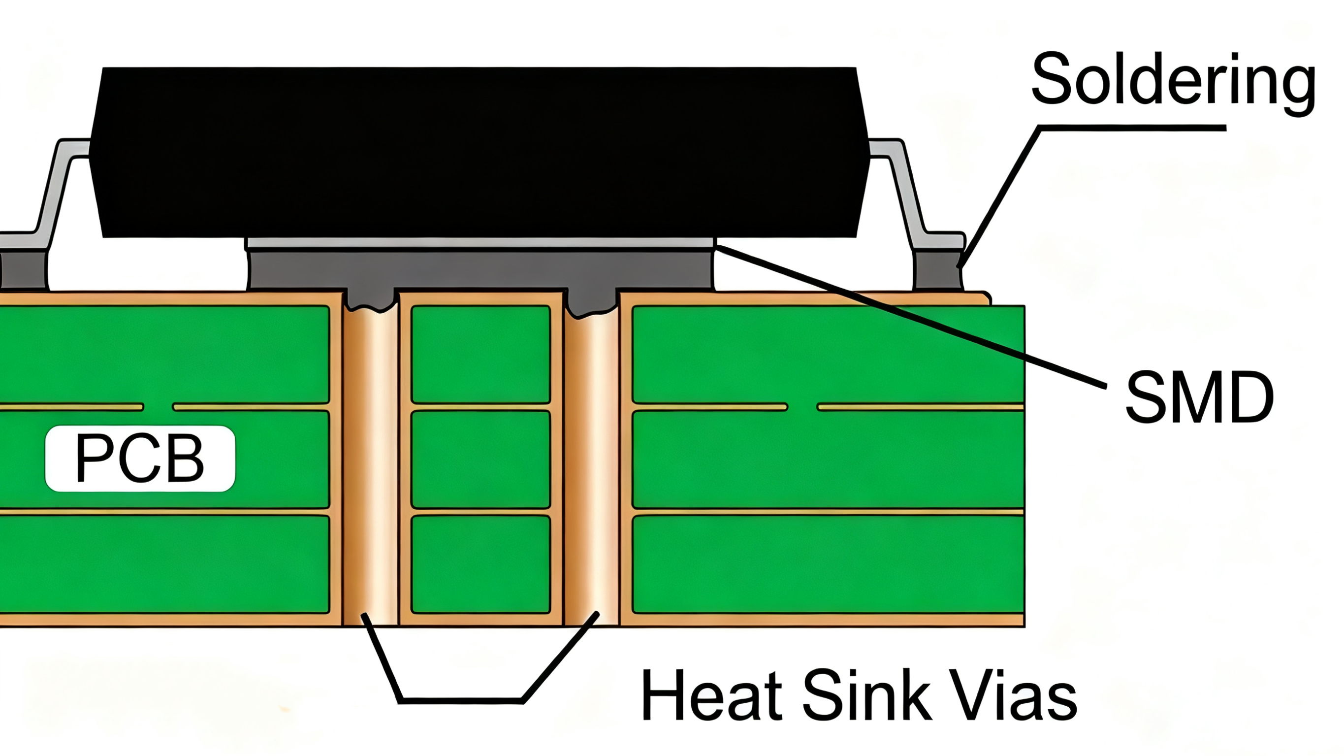
Thermal vias are critical for vertical heat conduction between copper layers. Proper via quantity, density, and structure can dramatically enhance PCB vertical heat transfer.
More vias typically improve heat dissipation, but manufacturing cost and signal integrity must be considered. Avoid placing vias near high-speed traces.
For low-power ICs, use vias with a diameter of 0.3–0.5 mm and spacing of around 1 mm. For high-power devices, apply an array layout such as 3×3, 4×4, or larger, depending on the thermal load.
However, through-hole vias directly under solder pads are not recommended, unless via-in-pad filled and capped technology is used. This prevents solder wicking during reflow, ensuring reliable solder joints and effective PCB thermal management.
The thermal performance of vias mainly depends on the copper plating thickness of the via walls, with a recommended plating thickness of ≥25 μm. Using a blind and buried via structure can also strengthen local heat conduction paths in inner layers. In manufacturing, filled vias or via-in-pad technology can be employed to create shorter and more efficient thermal paths.
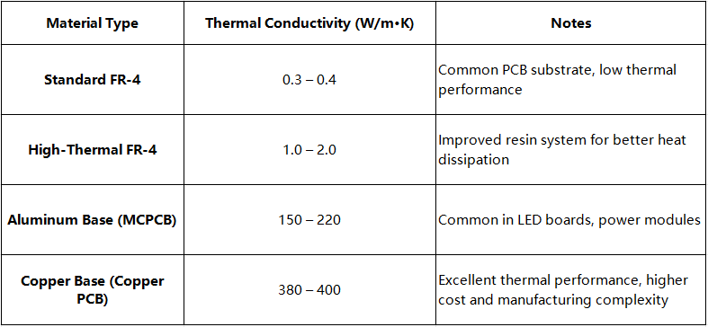
FR-4 is the most commonly used PCB substrate material, but conventional FR-4 has a relatively low thermal conductivity of 0.3–0.4 W/m·K. For improved PCB heat dissipation, designers can use high-thermal FR-4 (1.0–2.0 W/m·K), aluminum-based PCBs (150–220 W/m·K), or copper-based PCBs (380–400 W/m·K). Aluminum and copper substrates offer excellent thermal conductivity, effectively transferring heat from components to the overall thermal management structure.
Multilayer PCB stack-ups provide additional thermal diffusion paths. Placing large GND and Power planes in inner layers helps spread heat more evenly in the lateral plane, improving thermal design in PCB and reducing local hot spots.
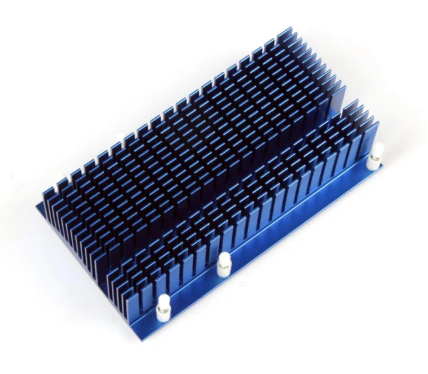
Heatsinks can be added to high-power components, such as power amplifiers or processors, to increase the heat transfer surface and improve PCB thermal management. When designing heatsinks, consider the contact area with air and surface treatments to enhance PCB heat dissipation efficiency.
Encapsulating the PCB or module with high-thermal-conductivity epoxy or silicone not only transfers heat from components to the enclosure more uniformly but also provides moisture protection, vibration resistance, and electrical insulation, supporting smart PCB design and long-term reliability.
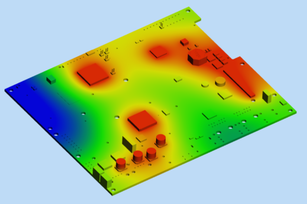
During the design phase, thermal simulation tools (such as ANSYS, SolidWorks Thermal, or Thermal Desktop) can model PCB heat distribution. Simulation helps identify potential hot spots and allows for optimization before fabrication, improving thermal management considerations.
Thermal imaging can measure real-world operating temperatures, providing accurate data for further design adjustments. This ensures more effective thermal design in PCB and validates the overall PCB layout thermal management strategy.
In PCB design, thermal management is not only crucial for device performance but also significantly affects overall system reliability. Designers should comprehensively consider heat generation mechanisms, material selection, component layout, copper plane design, and thermal simulation. By integrating these measures, smart PCB design can achieve effective PCB heat dissipation and thermal management, supporting higher-performance electronic products as technology continues to advance.
Feel free to contact us if you have any question.