Every step in the PCB design process is crucial to the success of the final product. A rigorous and efficient PCB design workflow ensures optimal functionality, performance, reliability, and cost-effectiveness. Professional design helps transform ideas into reality while reducing risks and saving time.
Clear requirements are the foundation of a successful project. In this stage of the PCB design process, our team collects and analyzes client needs, including:
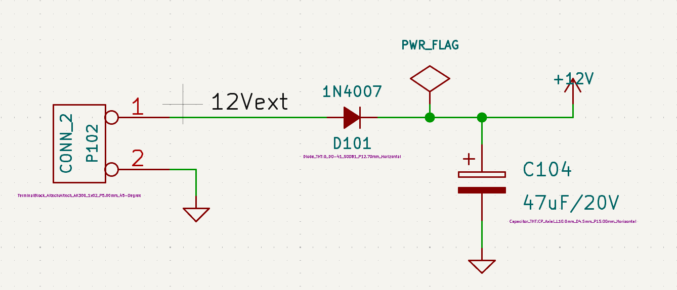
After confirming the concept, a functional block diagram is created and reviewed with the client. Once approved, schematic design begins. High-quality schematics reduce material waste, prevent rework, and improve overall efficiency in the PCB design process**.**
Key activities:
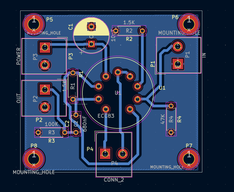
After schematic approval, we proceed with PCB layout design and routing. Proper layout ensures manufacturability and prevents defects. High-quality PCB layout reduces production errors and lowers long-term maintenance costs.
Key activities:
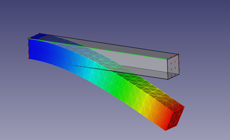
Design verification is a critical part of the PCB design process. It identifies potential issues before production, reducing costs and risk.
Key activities:
PCB prototyping and testing are a critical part of the design process and an essential step before mass production. Prototype testing validates the design and identifies potential problems early.
Typical prototype tests include:
Some hardware functions require software to operate. Firmware development begins after schematic approval and continues alongside PCB prototyping for integrated testing.
Key activities:
For clients needing enclosures, enclosure design can run in parallel with PCB layout design.
Key activities:
After prototype testing is complete, we first send the samples to the client for inspection. Once the prototypes are approved, mass production can proceed. During this stage, our design team works closely with the PCB manufacturer to ensure the design is successfully translated into high-quality finished boards, providing rapid feedback and solutions for any production issues that may arise.
Considerations include:

(Flowchart)
High-quality PCB design is the foundation for product success. From requirement analysis, schematic capture, PCB layout design, verification, prototyping, to mass production preparation, each step is essential. PCBWay professional team ensures your ideas become reality while minimizing risk, saving costs, and shortening time-to-market.


