Understanding EMI, EMS, and EMC in PCB Design
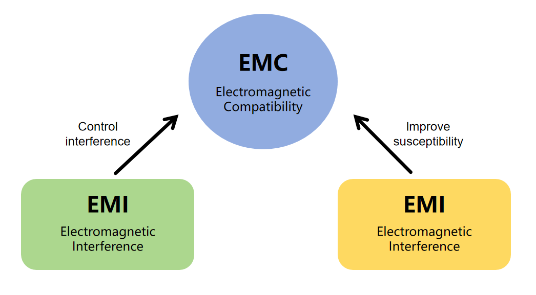
EMI (Electromagnetic Interference) refers to the harmful electromagnetic noise emitted by electronic products during operation, which can interfere with other devices. It is essentially electromagnetic "pollution" generated by equipment and must be controlled within certain limits.
EMS (Electromagnetic Susceptibility / Immunity) is the ability of a device to resist external electromagnetic interference. It measures how immune the device is to electromagnetic “attacks” from its environment.
EMC (Electromagnetic Compatibility) = Low EMI + High EMS. It represents a device’s overall capability, which includes two aspects:
Firstly, its EMI emission level is sufficiently low so that it does not interfere with other devices.
Secondly, it has good EMS (also called immunity), meaning it can withstand or be immune to disturbances from the surrounding electromagnetic environment while maintaining normal performance.
Therefore, EMC is the fundamental guarantee of product functional stability.
Design Guidelines for EMC Optimization
How to reduce EMI and improve EMS in design to enhance EMC — the PCBWay design team generally starts from the following four aspects:
1. Signal Integrity and High-Speed Routing
The common goal of these three practices is to ensure that signals travel from the transmitter to the receiver with intact waveforms, accurate timing, and without generating excessive electromagnetic interference (EMI).
1.1 Proper Routing to Maintain Signal Integrity
- Impedance Control: High-speed signal traces must be designed based on the stack-up structure through characteristic impedance calculation (typically 50 Ω single-ended, 100 Ω differential; the exact value should be chosen according to the interface standard such as USB, PCIe, LVDS, etc.). Impedance is kept uniform and continuous by controlling trace width, dielectric thickness, and dielectric constant. Any impedance discontinuity can lead to signal reflections, causing waveform overshoot, ringing, and distortion. For impedance calculation, you can use the PCBWay Impedance Calculation Tool.
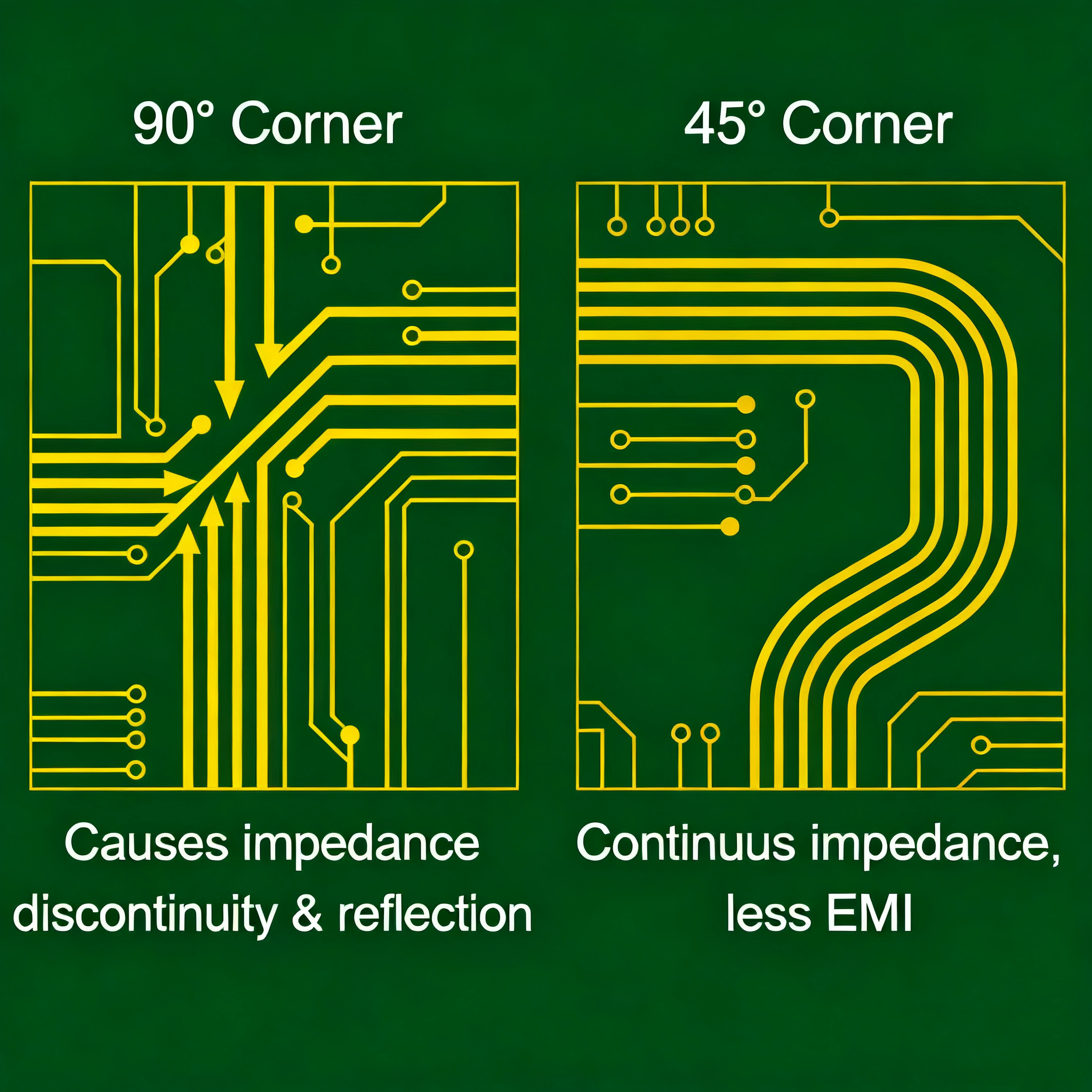
- Avoid Sharp Corners: Signal traces should use 45° bends or arc-shaped turns instead of 90° corners. Right-angle routing increases parasitic capacitance, causes impedance discontinuities, and can act as a potential radiation source.
- Short and Straight Paths: As long as timing requirements are met, traces should be kept as short as possible to reduce transmission delay and signal attenuation.
1.2 Differential Pair Routing and Guard Trace Techniques
Differential signaling is a powerful method to ensure signal integrity and improve noise immunity.
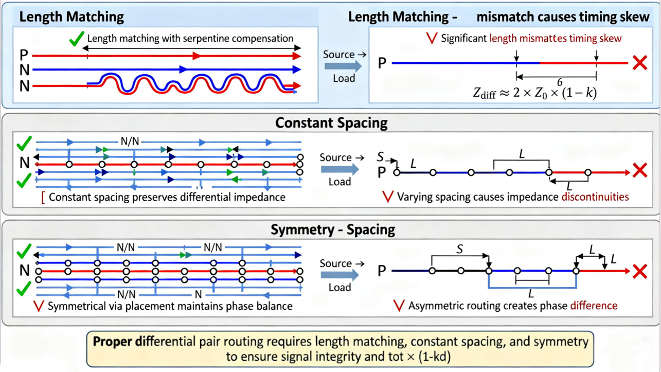
Differential Pair Routing:
- Length Matching: The two traces of a differential pair (P and N) must be kept as equal in length as possible. Any mismatch can cause timing skew and common-mode noise, which reduces noise immunity. Fine-tuning is usually achieved using serpentine routing.
- Constant Spacing: The two traces should maintain a uniform spacing throughout the entire path from driver to receiver, in order to preserve differential impedance.
- Symmetry: Routing should be as symmetrical as possible, avoiding mismatched vias or inconsistent layer transitions, which could introduce phase differences.
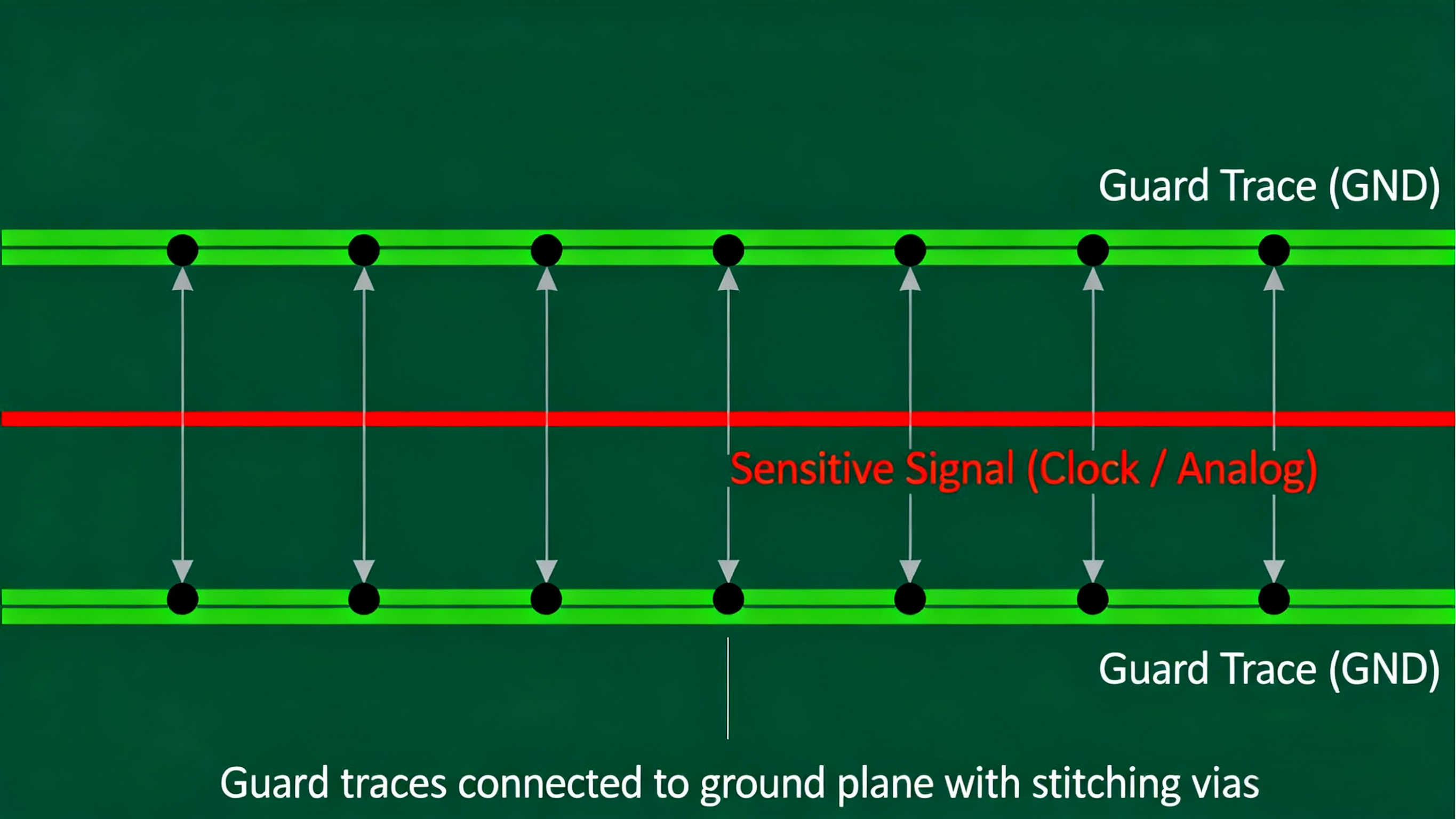
Guard Trace Technique (Guarding):
- Purpose: Used to isolate sensitive signal traces (such as high-impedance analog lines or clock lines) and prevent interference from nearby aggressor signals. The guard trace itself must have a proper return path to the ground plane; otherwise, it may become a source of interference instead.
- Method: Route ground traces in parallel on both sides of the sensitive signal, and place stitching vias frequently along the guard trace to connect it to the main ground plane. This creates a “trench” around the signal line, effectively shielding it from external noise. Again, the guard trace must be tied to ground to ensure a proper return path.
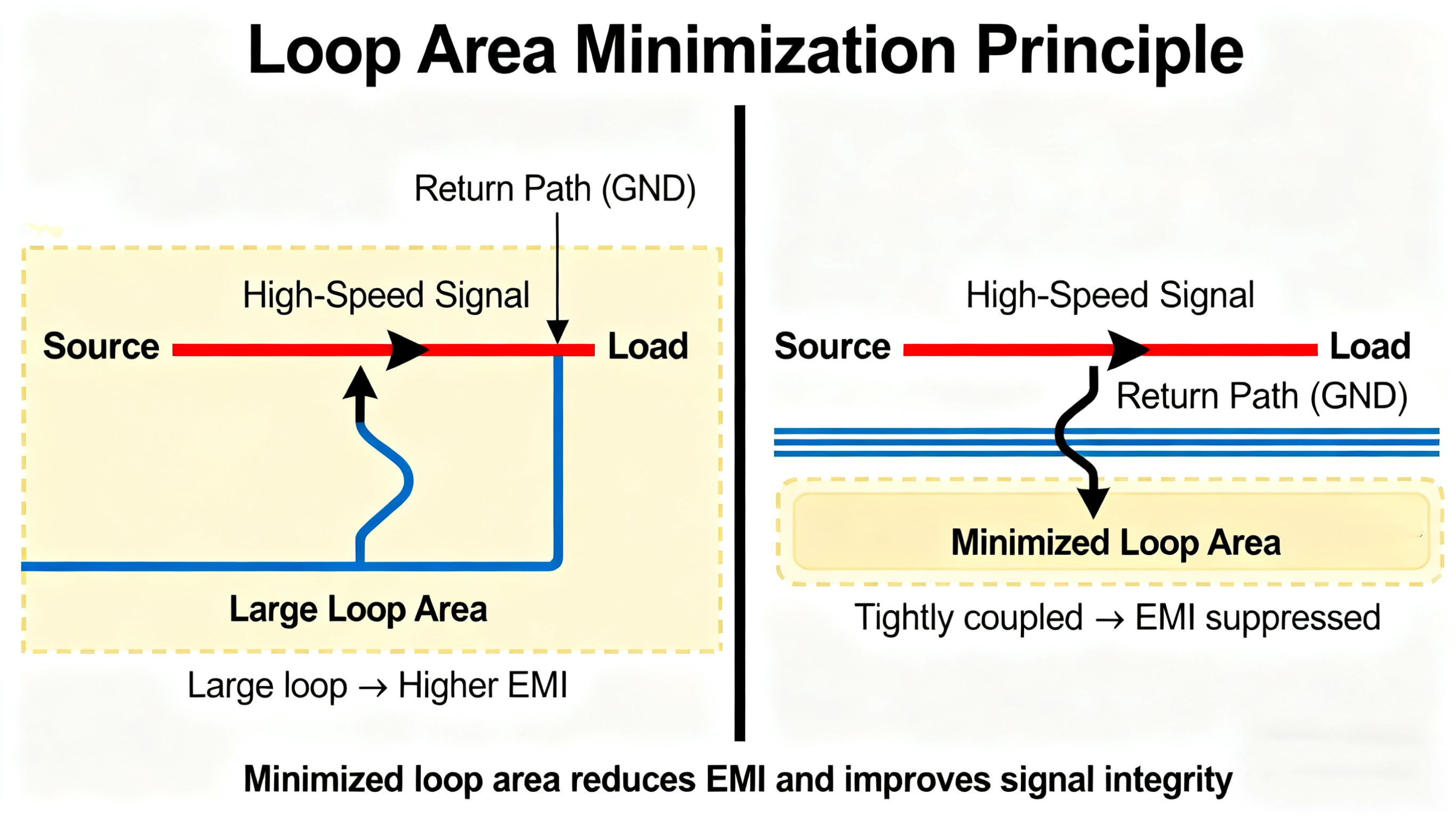
1.3 Minimizing Loop Area and Crosstalk
This is a core principle in suppressing EMI.
Minimizing Loop Area:
- Principle: According to electromagnetic theory, current always flows in a closed loop. The larger the loop area, the stronger its equivalent antenna effect, leading to higher electromagnetic radiation and greater susceptibility to external interference.
- Implementation: Always provide the shortest, continuous, and unbroken return path for signals. The return current of high-speed signals flows tightly beneath the signal trace along the reference plane (ground or power). Therefore, the reference plane must not be arbitrarily split, ensuring an unobstructed return path. This is the most effective way to minimize loop area.
Minimizing Crosstalk:
- Principle: Crosstalk is unwanted noise coupled from one network to another adjacent network through mutual capacitance and inductance.
- 3W Rule: To effectively reduce crosstalk, the edge-to-edge spacing between parallel traces should be at least three times the trace width (3W).
- Increase Spacing: Enlarging the spacing further is the most straightforward way to reduce crosstalk.
- Reduce Parallel Length: Minimize the length of parallel routing between signal traces whenever possible.
- Ground Shielding: Place a ground trace between two sensitive signal lines that must run in parallel; this can effectively isolate them.
Proper routing forms the foundation. Differential pair routing is a more advanced technique for achieving highly reliable transmission. Their combined outcome and ultimate goal is to minimize loop area and crosstalk, thereby ensuring signal integrity (SI) while also addressing electromagnetic compatibility (EMC).
2. Power and Ground Design
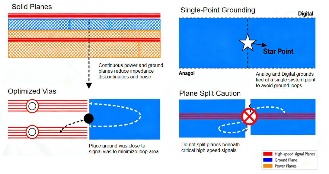
2.1 Ground and Power Plane Design
- Prioritize Solid Planes: Use continuous power and ground planes in multilayer boards to reduce impedance discontinuities and noise coupling.
- Multi-Point vs. Single-Point Grounding: Analog and digital circuits are typically partitioned and should be tied together at a single system point to avoid ground loop interference.
- Optimized Power/Ground Vias: High-frequency return current paths should be as short as possible. Place ground vias close to signal vias to reduce loop area.
- Caution with Plane Splits: Do not arbitrarily split power or ground planes beneath critical high-speed signals, as this may disrupt the signal’s return path.
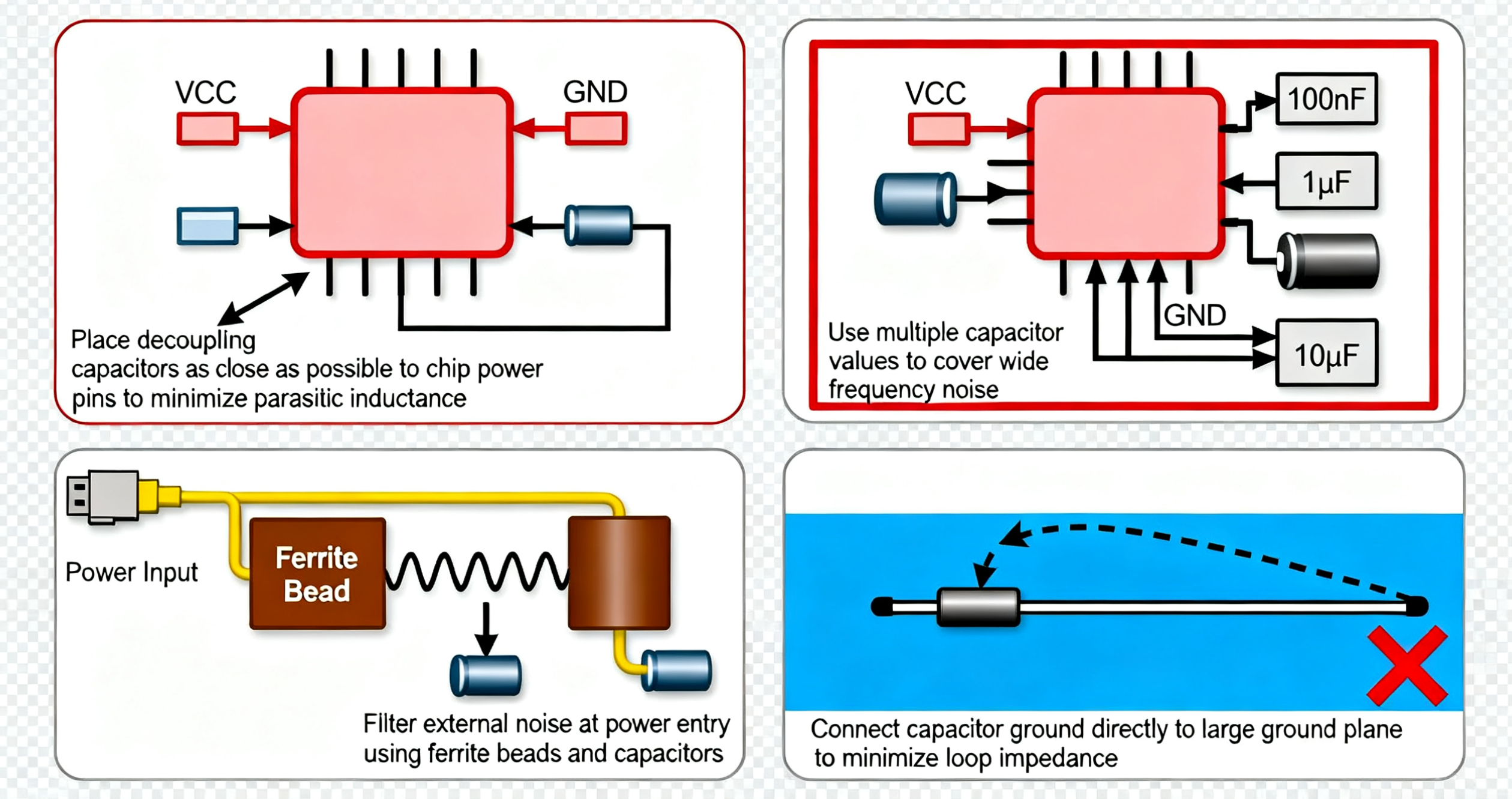
2.2 Placement of Decoupling and Bypass Capacitors
- Close to Chip Power Pins: Decoupling capacitors must be placed as close as possible to the chip’s power and ground pins to minimize parasitic inductance.
- Multiple Capacitance Values: Use a combination of capacitors with different values (e.g., 100 nF, 1 µF, 10 µF) to cover noise across a wide frequency range.
- Power Entry Filtering: At the power entry, add ferrite beads or common-mode chokes together with capacitors to form a low-pass filter, suppressing external noise from entering.
- Direct Ground Connection: The ground terminal of capacitors should connect directly to a large ground plane to minimize loop impedance.
3. Component Placement and Shielding
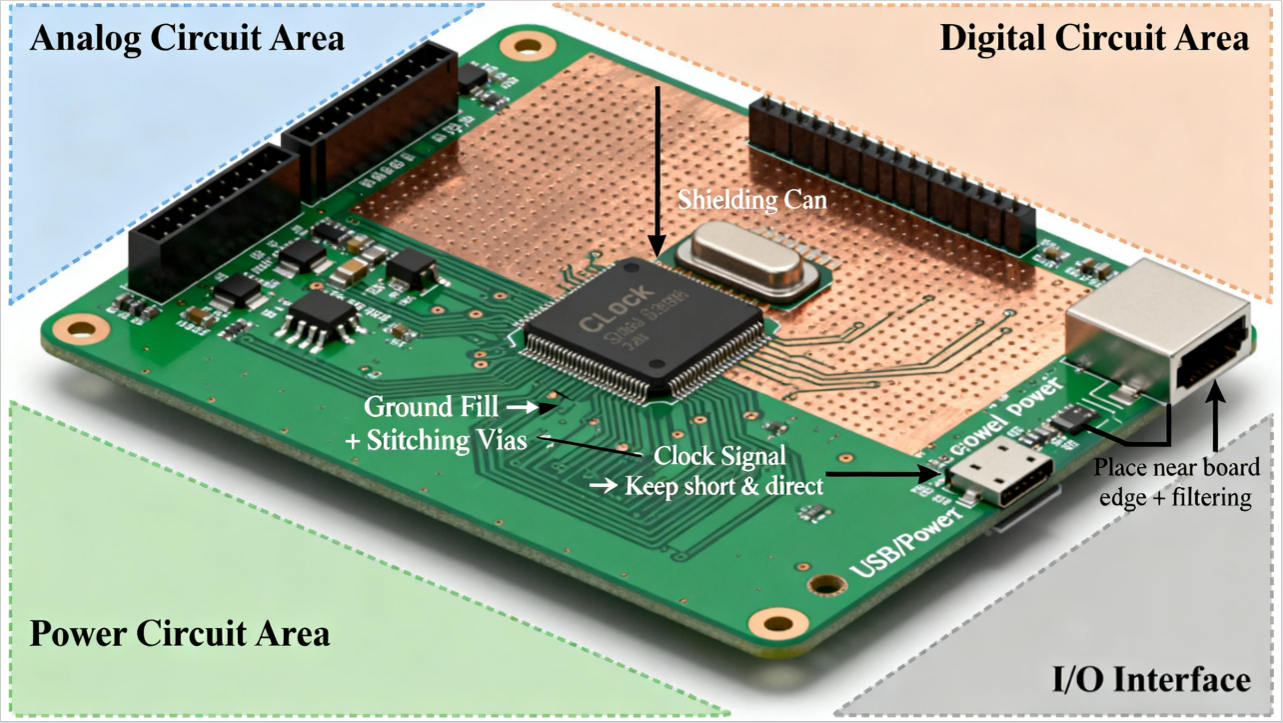
3.3 Optimized Component Placement to Reduce EMI
- Functional Partitioning: Separate analog and digital circuits to prevent high-speed switching noise from coupling into sensitive analog circuitry. Power circuits and clock circuits should also be partitioned independently to reduce mutual interference.
- Prioritize Critical Signals: Place clocks, high-speed differential pairs, and RF modules as close as possible to their associated chips. Keep routing short and direct to minimize antenna effects.
- Ground Fill: Fill unused board areas with grounded copper, and connect them to the ground plane through multiple vias to form a “shielding wall” that suppresses EMI radiation.
- Shielding Cans and Physical Isolation: For sensitive circuits such as RF front-ends and clock sources, use metal shielding cans or dedicated isolation zones on the PCB to reduce internal and external coupling.
- I/O and Power Interface Placement: Place external connectors near the board edge with clear signal entry/exit paths to avoid long crossing traces. Power input ports should preferably integrate filtering components.
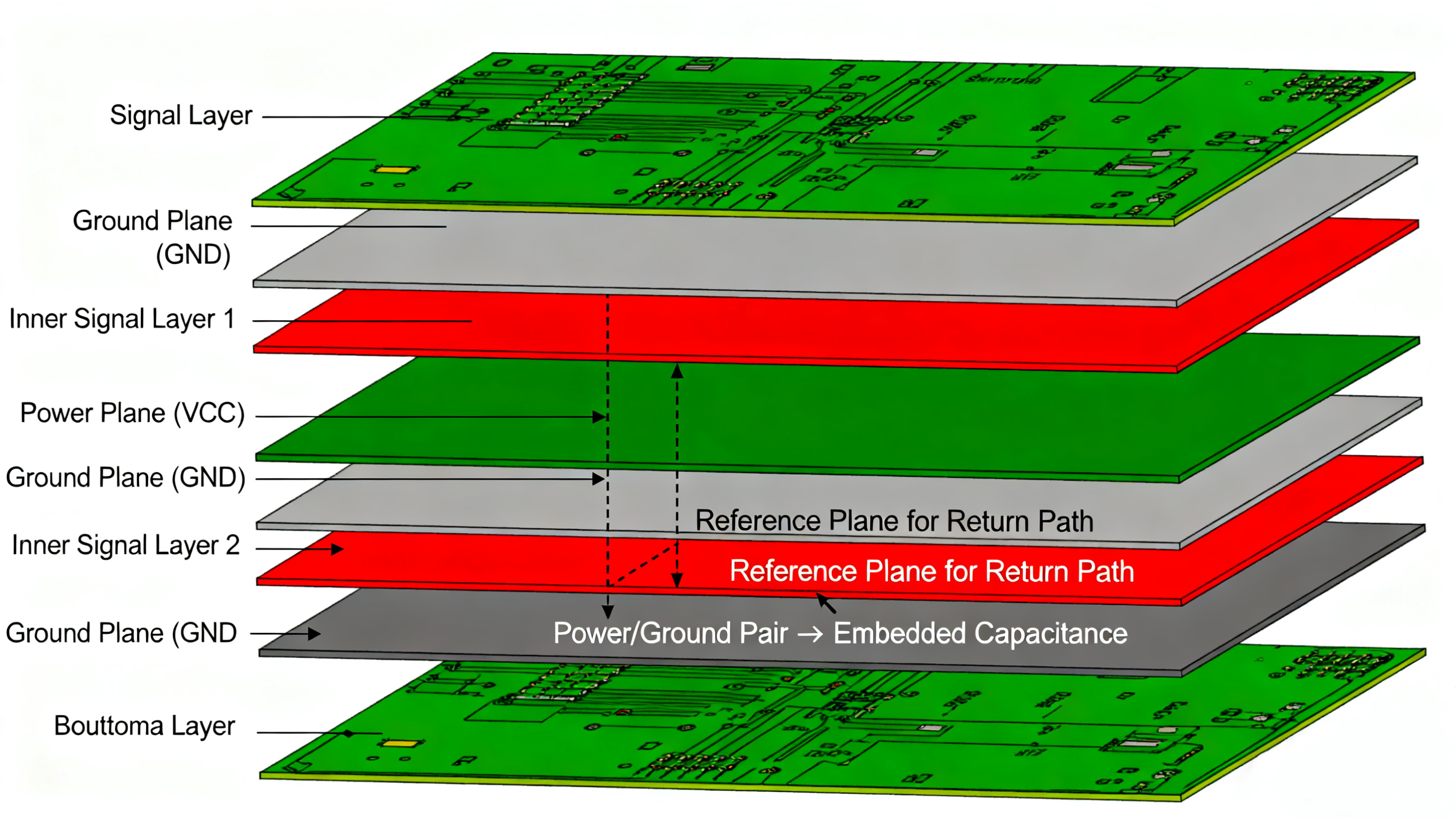
4. PCB Stack-Up Optimization
4.1 Optimizing PCB Layer Structure
- Choose the Right Number of Layers: High-speed designs typically use 4 or more layers. A common 4-layer structure is Signal–Ground–Power–Signal. For more complex high-speed designs, 6 or 8 layers (or more) are often preferred for better signal integrity and EMC performance.
- Adjacent Signal and Reference Layers: High-speed signal layers should be placed adjacent to continuous ground or power planes to ensure a proper return path, reducing loop area and EMI.
- Symmetry Between Power and Ground Planes: When power and ground planes are placed adjacent, they form a parallel-plate capacitor that helps filter high-frequency noise and improves power integrity.
- Avoid Routing Over Split Planes: Do not route high-speed traces across splits in power/ground planes, as this interrupts the return path and can cause radiation and crosstalk.
- Stack-Up Impact on Impedance: Impedance control depends on dielectric thickness, dielectric constant, and trace width. A well-planned stack-up simplifies impedance design and improves manufacturability.
Testing and Compliance
Early EMI pre-compliance testing helps identify potential issues before formal certification, saving both time and cost. We also ensure that designs follow recognized EMC standards (such as FCC, CE, and CISPR) to guarantee that products can enter global markets smoothly.
Following the EMC design guidelines above can significantly reduce signal interference and compliance risks. PCBWay professional design team is well-versed in high-speed signal and EMI/EMC design standards, and can provide tailored solutions early in the project to help reduce debugging time and potential risks.
Feel free to ask us if you have any question.


